Advanced Semiconductor Packaging Technologies: The Development Trend and the Growth Drivers, IDTechEx Reports
Comunicato Precedente
Comunicato Successivo
The shift from 2.5D hybrid integration to complete 3D vertical integration is crucial for future data-centric applications, and in this article, we will focus on this transition.
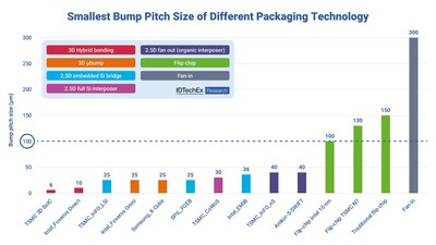
The primary challenge in the shift from 2.5D to 3D is to scale the size of the bumping pitch. In a 2.5D IC package, the bump pitch size ranges between 25 µm and 40 µm, depending on the interposer material. However, for a 3D stacking package, the bump size must be scaled down to a single digit µm or even lower down to below 1 µm dimension. TSMC has reported that the bump pitch for stacking N7/N6 chips is 9 µm and 6 µm for N5 chips stacking. This is expected to further decrease to 4.5 µm for N3 chip stacking and continue to decline for future generations of ICs. Stacking two chips with a small bump pitch size poses a significant challenge, as high-precision alignment on bonding dielectric materials must be achieved, especially at low temperatures. Additionally, proper control of Cu filling materials is necessary to prevent overflow during the bonding process. Furthermore, thermal management becomes a critical issue for packages with small bumping scales, which necessitates the consideration of package designs that enable better heat transmission and possible liquid cooling technologies.
The Growth Drivers
IDTechEx has identified four main application areas for advanced semiconductor packaging: high-performance computing (HPC) applications/data centers, communication networks, autonomous cars, and consumer electronics. The increasing demand for data processing is the primary driving force behind the growth in these application areas. However, each application has specific requirements that necessitate different advanced semiconductor packaging technologies.
For HPC applications/data centers, the priority is to provide superior data processing capabilities, making 2.5DIC technologies that use Si interposer or Si bridge the preferred option, despite their higher cost. In contrast, consumer electronics such as smartphones or smartwatches focus on miniaturization and cost, with organic-based packaging technologies being the top choice.
In 5G and beyond communication, the key challenge is transmission loss. Hence, advanced packaging technologies are used to bring the antenna closer to the RF IC chip, minimizing transmission loss. "Antenna-in-package (AiP)" is currently the most viable option for 5G mmWave, while "Antenna on chip/wafer (AoP)" is still under intense development to reduce costs.
For future autonomous vehicles, heterogeneous integration of CPUs and other components, such as HBM and reliable power delivery systems, will create new opportunities for advanced semiconductor packaging and innovation.
The expansion of data processing is the unifying growth factor for all these applications. However, as the requirements for each application area differ, advanced semiconductor packaging technologies are being used to meet specific needs.
IDTechEx has released a new market research study titled "Advanced Semiconductor Packaging 2023-2033". This study examines the market prospects, key player analysis, and most recent developments in advanced semiconductor packaging technologies. This report also conducts a comprehensive examination of the semiconductor market as a whole. Additionally, IDTechEx leverages its expertise and years of research in data centers, autonomous vehicles, 5G, and consumer electronics to provide the reader with a thorough understanding of how advanced semiconductor packaging is influencing various industries and what the future may hold.
To find out more about this IDTechEx report, including downloadable sample pages, please visit www.IDTechEx.com/ASP.
IDTechEx's market research is differentiated through the primary information gathered, technical depth, and unbiased appraisals. IDTechEx covers a wide range of topics and helps understand the industry's pain points and unmet needs. For more information, please visit www.IDTechEx.com/research.
About IDTechEx
IDTechEx guides your strategic business decisions through its Research, Subscription and Consultancy products, helping you profit from emerging technologies. For more information, contact [email protected] or visit www.IDTechEx.com.
Images download: https://www.dropbox.com/scl/fo/r8pxryke1fpswtsvj4b23/h?dl=0&rlkey=0hzvd526fjgksq7w5qvr4gy1k
Media Contact:
Lucy Rogers
Sales and Marketing Administrator
[email protected]
+44(0)1223 812300
Social Media Links:
Twitter: www.twitter.com/IDTechEx
LinkedIn: www.linkedin.com/company/IDTechEx
Facebook: www.facebook.com/IDTechExResearch
Photo: https://mma.prnewswire.com/media/2076779/Bump_Pitch_Size_of_Different_Packaging_Technology.jpg
Logo: https://mma.prnewswire.com/media/478371/IDTechELogo.jpg
![]() View original content:https://www.prnewswire.co.uk/news-releases/advanced-semiconductor-packaging-technologies-the-development-trend-and-the-growth-drivers-idtechex-reports-301824329.html
View original content:https://www.prnewswire.co.uk/news-releases/advanced-semiconductor-packaging-technologies-the-development-trend-and-the-growth-drivers-idtechex-reports-301824329.html


